About Group
About Group


Material Property Metrology Group accurately predicts next-generation materials that are highly likely to be utilized in future advanced, applied devices and standard quantum devices by using AI-based material discovery algorithms and first-principles calculation methods.
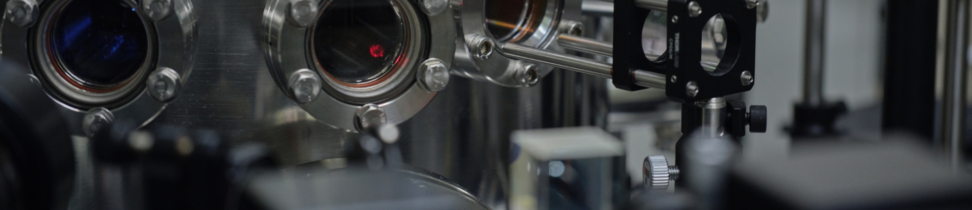
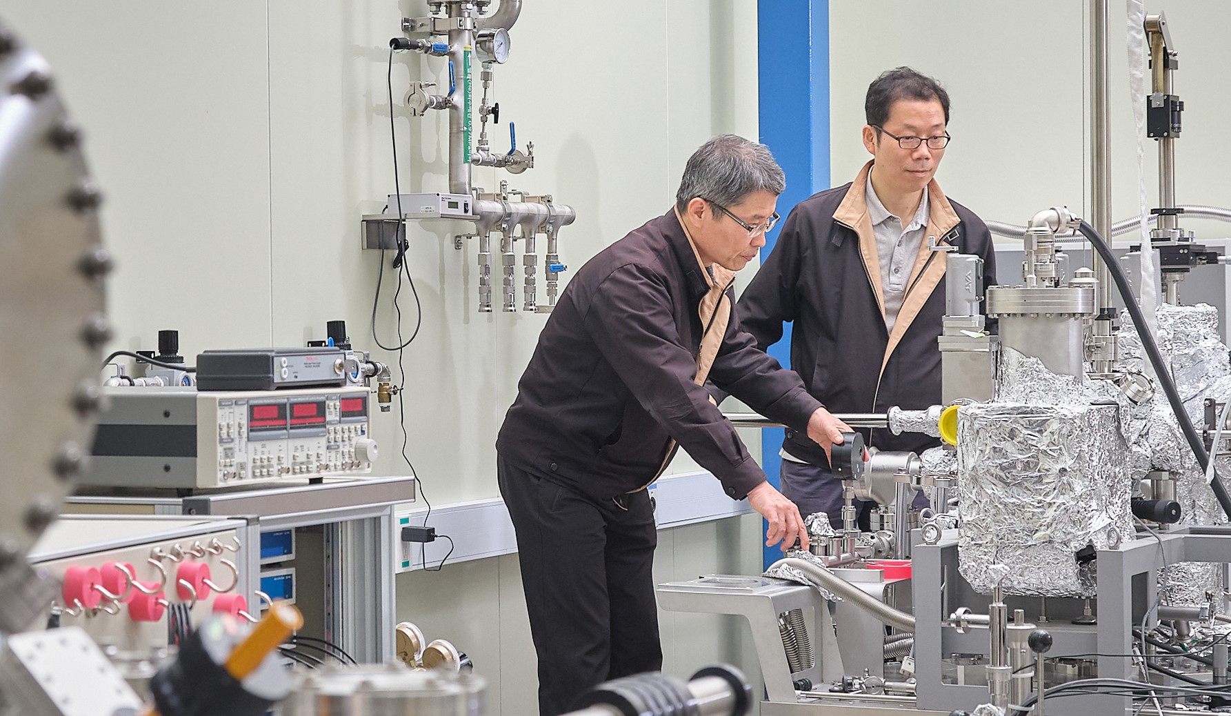
We are developing new measurement platforms and technology to measure the diverse properties of future materials, obtained through the synthesis of high-purity materials, with high reliability and accuracy at the single-atom level in the microscopic domain.
Current R&D Projects
-
 1
Development of technology for design and exploration of hyperfunctional materials using global optimization algorithms based on big data-powered AI
1
Development of technology for design and exploration of hyperfunctional materials using global optimization algorithms based on big data-powered AI
-
 2
Prediction of diverse basic properties of next-generation materials using first-principles calculations and computational simulation technology
2
Prediction of diverse basic properties of next-generation materials using first-principles calculations and computational simulation technology
-
 3
Development of ultra-high vacuum low-temperature scanning tunneling microscopy, variable-temperature atomic force microscopy, and photo-induced force microscopy for precise measurement of various composite properties of advanced materials
3
Development of ultra-high vacuum low-temperature scanning tunneling microscopy, variable-temperature atomic force microscopy, and photo-induced force microscopy for precise measurement of various composite properties of advanced materials
-
 4
Development of technology for electronic structures of advanced materials, optoelectronic and thermoelectric properties, thickness measurement of ultra-thin film and its compositional analysis, as well as establishment of standard measurement methods
4
Development of technology for electronic structures of advanced materials, optoelectronic and thermoelectric properties, thickness measurement of ultra-thin film and its compositional analysis, as well as establishment of standard measurement methods
-
 5
Development and measurement of next-generation advanced, applied devices and standard quantum devices using semiconductor manufacturing technology
5
Development and measurement of next-generation advanced, applied devices and standard quantum devices using semiconductor manufacturing technology
Recent R&D Highlights
- Development of methods for designing material property based on evolutionary learning and methods for data-based exploration of crystal structure using artificial neural networks
- Improvement of precision of device-based planar junction tunneling spectroscopy
- Development of surface chemistry analysis technology for single nanoparticles using photo-induced force microscopy
- Measurement/examination of lattice instability and electronic structure changes due to single-atom-level Kekulé distortion
- Development of technology for measurement and certification of absolute thickness of high-k ultra-thin oxide films
QUICK MENU
QUICK MENU 원하시는 서비스를 클릭하세요!
등록된 퀵메뉴가 없습니다.