About Group
Strategic Technology Research Institute Researchers
About Group


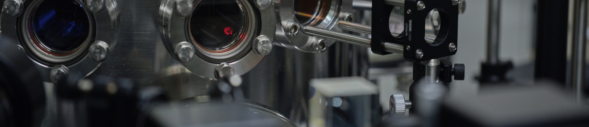
Semiconductor and Display Metrology Group conducts measurement science and technology research for semiconductors and displays. Based on these measurement technologies, we aim to contribute to the sustainable growth of national strategic technologies by providing real-time diagnostics for advanced device manufacturing processes, measurement of optical properties and operando, development of semiconductor sensors for compound and advanced 2D materials, and performance evaluation services for materials, parts, and equipment used in advanced device manufacturing processes.
Current R&D Projects
-
 1
Development of process monitoring sensor technology, including plasma density, contaminated particles, and carbon-neutral process diagnostics
1
Development of process monitoring sensor technology, including plasma density, contaminated particles, and carbon-neutral process diagnostics
-
 2
Development of measurement technology for optical properties and operando
2
Development of measurement technology for optical properties and operando
-
 3
Technology development for basic performance evaluation of materials, parts, and equipment for advanced semiconductor and display device manufacturing processes
3
Technology development for basic performance evaluation of materials, parts, and equipment for advanced semiconductor and display device manufacturing processes
-
 4
Development of process technology for high-quality compound semiconductors and novel 2D semiconductor materials
4
Development of process technology for high-quality compound semiconductors and novel 2D semiconductor materials
Recent R&D Highlights
- Development of certified reference materials for thin film thickness of 300 mm
- Establishment of comprehensive performance evaluation infrastructure and measurement services for next-generation vacuum materials, parts, and equipment
- Analysis technology for organic thin films with depth resolution below 8.3 nm for OLED applications
- Development of sensors for simultaneous detection in the near and mid-infrared ranges using high-quality compound semiconductors, as well as development of infrared hyperspectral imaging sensors
- Development of measurement standards for radiative forcing calculation for climate warming index
QUICK MENU
QUICK MENU 원하시는 서비스를 클릭하세요!
등록된 퀵메뉴가 없습니다.