News & Updates
News & Updates
KRISS Establishes International Standard for the Thickness Measurement of Semiconductor Oxide Film
- Writerkrissadmin
- Date2021-05-03 00:00
- Hits11591
KRISS Establishes International Standard
for the Thickness Measurement of Semiconductor Oxide Film
- Using a measurement equipment from a domestic SME manufacturer,
providing a standard for the precise sub-nanometer measurement -
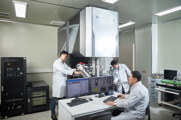
▲ The KRISS Surface Analysis Team conducting ultra-thin film measurement
The Korea Research Institute of Standards and Science (KRISS, President Hyun-Min Park) succeeded in establishing an international standard for the thickness measurement of semiconductor oxide films below 1 nanometer (nm, one billionth of a meter), using advanced measurement equipment developed by a domestic SME.
Researchers at the Surface Analysis Team of KRISS demonstrated for the first time in the world that medium energy ion scattering spectroscopy(MEIS), a technology manufactured in Korea, could be used to determine the absolute thickness* of semiconductor oxide films measuring less than 1 nm.
○ This technology is being to be used as an international standard, having been accepted as the method to determine the reference thickness of hafnium oxide films at an international meeting of CCQM.
* Absolute thickness: Actual thickness, which is not affected by other elements, in contrast to relative thickness.
The key point of this outcome is that the key measurement technology for the manufacturing process of semiconductor devices was established using domestically manufactured advanced measurement equipment. This result will assure the highest level of measurement reliability to the domestic semiconductor manufacturers and their technical superiority over the competitors in other countries will be further enlarged.
The control of thin and uniform oxide films on the substrate is very important in the manufacturing process of semiconductor integrated circuit. The oxide film plays a core function for the electronic properties and circuit design of semiconductor by protecting the surface and controlling the movement of electrons.
Until now, oxide film thickness has been measured using technologies such as transmission electron microscopy (TEM), spectroscopic ellipsometry (SE), X-ray reflectivity (XRR), and so on. However, it was a big problem that the measured thicknesses by those methods significantly differed from the real thicknesses of the oxide films.
The surface analysis team of KRISS demonstrated that X-ray photoelectron spectroscopy (XPS), which had been used as the standard method for the thickness measurement of semiconductor oxide film, could not be used as a measurement standard and suggested MEIS as an alternative technique.
○ From a systematic comparison study for the thickness measurement, the team elucidated that the reference for thickness determination does not change in MEIS, unlike XPS.
MEIS is suitable for the analysis of composition, distribution, crystal structure and thickness of nanometer grade thin films with atomic layer depth resolution. Therefore, MEIS developed by a domestic SME can be used as important measurement equipment for the fabrication processes of advanced devices such as semiconductor.
MEIS was recognized as the new standard method for the thickness measurement of nanometer thin films in a pilot study jointly conducted with the Consultative Committee for Amount of Substance: Metrology in Chemistry and Biology (CCQM) under the International Committee for Weights and Measures (CIPM). Due to a critical problem in the determination of reference thicknesses using XPS, the reference thicknesses were decided by MEIS from a discussion between the experts of national metrology institutes around the world.
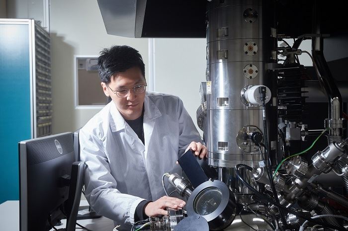
▲ A researcher from the KRISS Surface Analysis Team conducting ultra-thin film measurement
Principal Research Scientist Kyung Joong Kim of KRISS explained, “the significance of this study is that the performance of a domestic advanced equipment for the measurement of the absolute thickness of semiconductor oxide films to an ultra-precise level was successfully confirmed” and emphasized “we will do our best to contribute to enhancing the productivity of domestic companies by increasing the yield of next-generation semiconductor devices.”
The result of this study, funded by the National Research Council of Science & Technology’s Creative Convergence Research Projects, was published in Applied Surface Science (IF: 6.182), a leading international journal in the field of metrology.
QUICK MENU
QUICK MENU 원하시는 서비스를 클릭하세요!
등록된 퀵메뉴가 없습니다.