News & Updates
News & Updates
Device for extreme environments… key lies in single material diode
- Writerkrissadmin
- Date2019-01-22 00:00
- Hits11317
Device for extreme environments… key lies in single material diode
- High performance 2D diode made from a single material -
# A diode, which makes current flow in only one direction, is the most important device in modern electronic engineering. Usually, diodes are fabricated by heterojunctions between two different semiconductors, one p-type and the other n-type. Semiconductors are normally given p-type or n-type characteristics through a process called doping, which introduces impurities into the material. The devices attain various characteristics according to device structures and operation modes.
A high performance 2D diode with minimal energy loss that could work in extreme environments has been developed at the Korea Research Institute of Standards and Science.
Suyong Jung, Principal Research Scientist at the KRISS Quantum Technology Institute, and his team have successfully developed a vertical diode using just a single two dimensional semiconductor material of tungsten diselenide(WSe2)*, avoiding the conventional p-type and n-type heterojunction method. The technology has resolved problems in existing 2D devices, to offer outstanding performance and stability. In particular, it provides the best current density among currently existing 2D-based semiconductor devices, which means that it can transport the largest possible amount of charge carriers per unit area.
* Tungsten diselenide(WSe2): A transition metal dichalcogenide, which is a two dimensional layered material that can be separated into monolayer form. It possesses semiconductor properties, with the Fermi level located in the middle of its energy bandgap, making it relatively easy to induce p-type or n-type semiconductor characteristics through external doping.
Lately, active research fields have been focused on using 2D-layered semiconducting materials, which retain their semiconductor properties even at a single atomic layer thickness, aiming for high efficient electronic and optoelectronic devices.
Until now, conventional p-type and n-type heterojunctions have been implemented to build 2D layered semiconductor diodes. However, given the nature of 2D materials that are directly exposed to external disorders, the imperfect heterojunctions become one of the most critical components undermining 2D-based electronic device performances, resulting in lowering operation current partly due to enhanced Schottky barriers*, contact resistance due to physical/chemical defects, and unwanted dopings by incomplete junctions.
* Schottky barrier: Potential energy barrier occurring in the junction when a metal and a 2D semiconductor, or two different kinds of 2D semiconductors, are joined.
Principal Research Scientist Suyong Jung and his team successfully built a stable high performance diode using only tungsten diselenide(WSe2), a 2D layered semiconductor material. Although conventional methods are based on forming a heterojunction with two different materials, p-type and n-type semiconductors, the current study utilizes a metal-induced doping method to a single WSe2 crystal: introduce p-type and n-type semiconducting properties through direct metal depositions on the two respective ends of the WSe2 material.
The vertical diode developed by Jung’s team features an insulation layer that retains the original properties of WSe2, sandwiched between the p region and n region. By adjusting the length of the insulation layer, i.e. the thickness of the thin film, diodes with varying device characteristics can be created.
Another strength of this technology is that the underlying principle of charge transport in the diode relies on quantum tunneling*, which could be used in high-speed electronic device applications.
* Quantum tunneling: a quantum physics phenomenon, in which tiny particles such as electrons or atomic nuclei can pass through barriers of force fields.
“The vertical diode structure that we’ve developed has a simple device composition, and can be applied to not just WSe2, but a wide range of 2D materials,” says KRISS Principal Research Scientist Suyong Jung, adding “the diode can be used in sub-miniature devices that can withstand extreme environments, such as extreme heat, extreme cold, and extra high voltage, while minimizing energy loss. This makes it highly useful for future industrial applications such as ultrasensitive photodetectors”.
This study and its findings were published in the leading journal “Nature Communications” (IF: 12.124) in December, 2018.
○ Detailed description of research
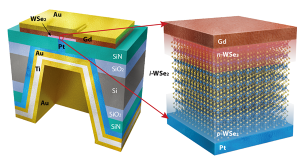

- KRISS Principal Research Scientist Suyong Jung and his team have built an experimental single crystal WSe2-based vertical diode using the WSe2 doping effect at the junction between the contact metal and WSe2, and have determined the WSe2 thin film thickness dependent quantum charge transport effect.
- The WSe2 optical·electronic device platform built using just a single 2D semiconductor material is not only simple to manufacture, but also resolves issues associated with existing p-n type semiconductor heterojunction device compositions, achieving measurement reliability and improvement for precise analysis of device characteristics.
- The team also found that the electron transport properties of the vertical WSe2 diode depended on a series of quantum charge transport phenomena such as direct tunneling, Fowler-Nordheim tunneling and Schottky emission effect, according to the thickness of WSe2.
- The vertical WSe2 diode developed in this study has device properties that can be controlled using just changes to the thickness of the WSe2 single crystals, while utilizing the strengths of both the Schottkey diode with high current capacity, and p-i-n diode with outstanding rectification properties, presenting the possibility of a highly efficient high performance semiconductor-based diode.
○ What sets this achievement apart?
Using just the singular WSe2 crystal semiconductor material, physical and chemical problems that arise in existing devices based on physical heterojunctions of p and n-type semiconductors are resolved.
As the device works on charge transport based on the quantum tunneling effect, it operates effectively even in extreme conditions such as ultrahigh vacuum and extreme cold.
○ What are its applications?
1. Demand for electronic devices that work under extreme conditions such as extreme heat, extreme cold, extra high voltage and high radioactivity will keep growing. The structurally stable vertical diode with quantum mechanics-based charge transport is expected to be more durable under extreme conditions compared to existing semiconductor-based electronic devices.
2. Solar power is a clean and renewable energy source, in which electricity is generated through light energy conversion. Solar cells are typically made using p-n semiconductor junctions. With this technology, solar cells with a sufficiently large light incident area but minimal energy loss through metal-semiconductor and semiconductor-semiconductor contact resistance can be fabricated, which presents a wide range of applicability to future industries.
![그림입니다. 원본 그림의 이름: 크기변환_[첨부2].jpg 원본 그림의 크기: 가로 1407pixel, 세로 925pixel 사진 찍은 날짜: 2019년 01월 04일 오후 10:36](/ease_src/crosseditor/binary/images/000002/20210924164627120_HDFHOTRV.jpg)
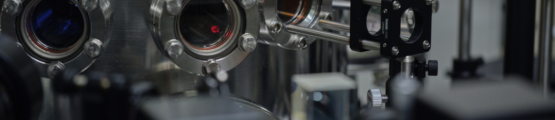
▲ KRISS Principal Research Scientist Suyong Jung (upper right) and his team are testing the electron transport properties of the diode.
![그림입니다. 원본 그림의 이름: 크기변환_[첨부3].jpg 원본 그림의 크기: 가로 1599pixel, 세로 965pixel 사진 찍은 날짜: 2019년 01월 04일 오후 10:40](/ease_src/crosseditor/binary/images/000002/20210924164627134_VJGR17FL.jpg)
▲ The KRISS team is preparing to conduct measurements of the vertical diode’s electron transport properties.
QUICK MENU
QUICK MENU 원하시는 서비스를 클릭하세요!
등록된 퀵메뉴가 없습니다.