Fabricating Infrared Device with Desired Characteristics by ‘Simply Heating’ in a Solvent
- Writerkrissadmin
- Date2021-12-22 00:00
- Hits618
Fabricating Infrared Device with Desired Characteristics
by ‘Simply Heating’ in a Solvent
- KRISS-KAIST joint research team developed a process
for intercalating organic ions to 2D layered materials.
- The technology may be applied to the development of sensors
for unmanned vehicles, gas detection, and COVID-19 body temperature sensing.
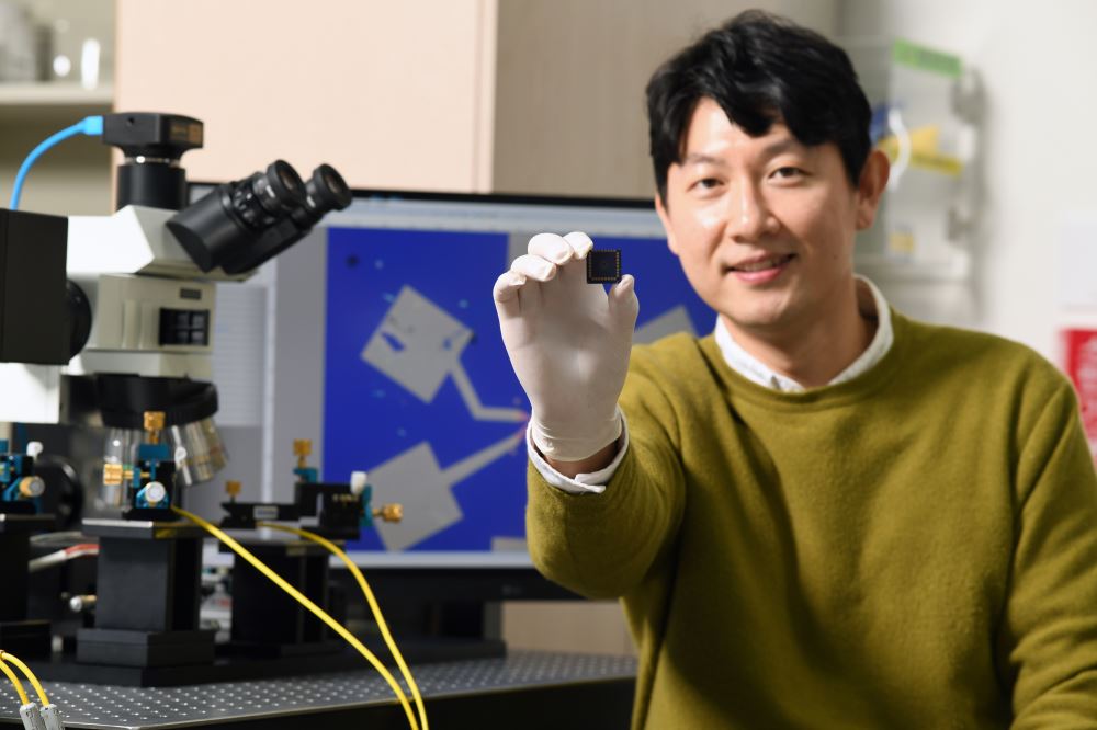
▲Seungwoo Song, a senior research scientist of the Interdisciplinary Materials Measurement Institute at KRISS,
is holding a photodetector fabricated by a method of simply heating.
KRISS successfully developed a new process that is applicable to the fabrication of next-generation infrared devices. The new technology can be used to fabricate devices at a price 1/100th of the previous process, and is also applicable to the manufacturing of flexible devices. Therefore, the technology has high potentials for application.
Infrared devices that are used in almost all the areas of Internet of Things (IoT) are drawing much attention, as they can be applied to various fields, including daily living, industries, healthcare, firefighting, and robots. Sensors manufactured by using an infrared device can detect human actions to automatically turn on and off the power of air conditioner, lighting, PC, TV and so on.
However, most of the conventional 2D layered semiconductor materials that have been used in the manufacturing of infrared devices have a bandgap* in the range of visible light, and chemically stable materials are rare. It is critical to control the bandgap, because it determines the light wavelength that can be detected by photodetectors** including infrared devices.
*Bandgap: The minimum energy that is needed to allow an electron from its confined state in a semiconductor or insulator
**Photodetector: A device that is fabricated to detect incident light of various wavelengths by converting into electric signals
Among the 2D materials, represented by graphene and molybdenum disulfide (MoS2), phosphorus black is capable of absorbing the light of the infrared wavelengths but it can hardly be applied to an infrared detector since its chemical stability is low and its bandgap is drastically changed depending on the number of layers. Ruthenium chloride, another 2D material, is drawing attention as a new material because its bandgap can be freely adjusted through electron doping.
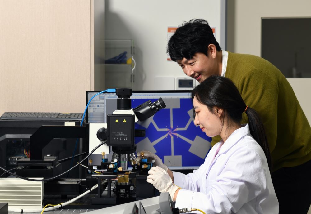
▲Researchers at KRISS are evaluating the performance of photodetectors.
The Operando Methodology and Measurement Team of the Interdisciplinary Materials Measurement Institute at KRISS conducted a joint study with Professor Kibum Kang’s group of the Department of Materials Science & Engineering at KAIST to develop a process for control the bandgap by a simple method of dipping the material into a solution and heating the mixture. The joint research team dipped 2D ruthenium chloride into a solution including organic ions and heated the resulting mixture intercalate organic positive ions to the vacancies between the layers of ruthenium chloride, controlling the bandgap through electron doping.
ㅇ The joint research team induced local charge doping in the vicinity of the transition metal by intercalating organic positive ions to ruthenium chloride, which is a Mott insulator having a strong repulsive force between the electrons.
As a result, the bandgap of ruthenium chloride was significantly reduced from 1.2 eV to 0.7 eV, indicating that the material can be applied to a device for detecting near-infrared.
The material can be used to absorb infrared having a wavelength of 1771 nm (nanometer, a billionth of 1 m), which is longer than the infrared that is currently detected (1033 nm). The bandgap of the material can be controlled in a simpler and more stable manner than before, and the photoreactivity is 50 times higher and the photoreaction rate is more than 3 times higher, compared with the pristine ruthenium chloride devices.
The cost of the process developed by the joint research team is as low as 1 hundredth of the conventional process. The biggest advantage of the newly developed process is that the resulting material has a smooth surface and thus can be applied to a flexible substrate-based flexible photodetector.
Seungwoo Song, a senior research scientist of the Interdisciplinary Materials Measurement Institute at KRISS, commented, “Our results can be widely applied to various kinds of 2D layered semiconductors, metals and nonconductors. We expect that the combination of various 2D layered materials and organic ions can improve the material properties and can be applied to the synthesis of highly useful new materials.”
The study was supported by the New Research Program of the Ministry of Science and ICT (MSIT) and the Key Research Program of KRISS. The results of the study were published online in ACS Nano (IF: 14.588), a globally renowned journal in the field of nanoscience, in November last year. Fin.