Looking into Nano-layered Structure of Semiconductor by a Single Shot
- Writerkrissadmin
- Date2022-02-11 00:00
- Hits1143
Looking into Nano-layered Structure of Semiconductor by a Single Shot
- The thickness and shape of a device are measured
in a nanometer scale by a nondestructive measurement method. -
- The technology is readily applicable to production sites. As the technology has already been transferred to a Korean company, commercialization of the technology is anticipated. -
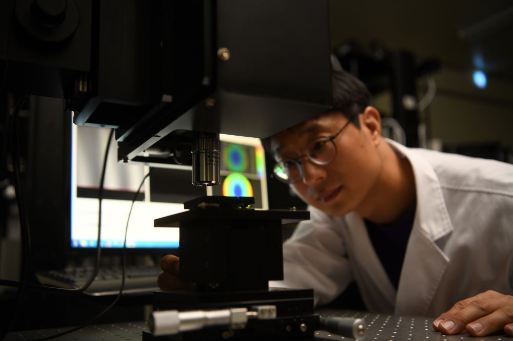
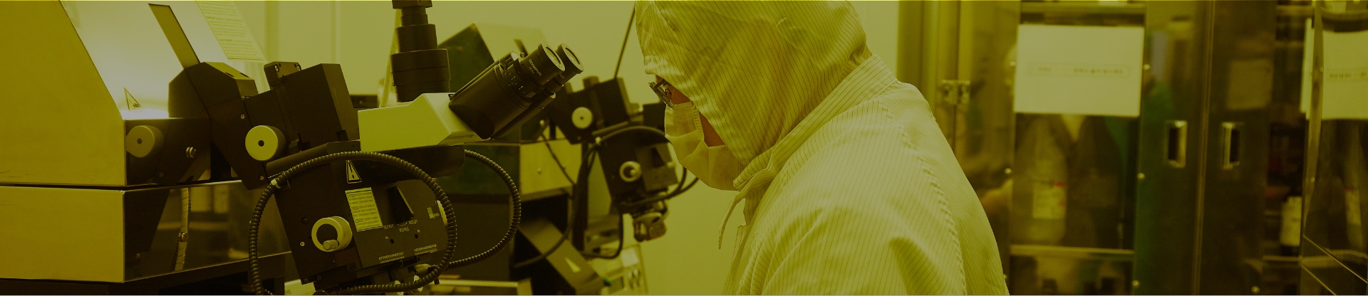
▲Dr. Young-sik Ghim, a principal research scientist of the Advanced Instrumentation Institute at KRISS,
is measuring a 3D nano device.
The Optical Imaging and Metrology Team at KRISS successfully performed one-shot, real-time inspection of internal device structure, including the structure of semiconductors, displays and sensors.
The highlight of the newly developed technology is that it allows for the measurement of both the thickness and shape of individual internal layers in a nondestructive measurement method without cutting a device. While the real-time nano-device measurement technology, developed by KRISS in 2020, employed a point measurement method and thus could be limitedly applied to thickness measurement, the newly developed technology allows for real-time measurement of both thickness and shape and thus is expected to have higher applicability.
The new technology can be used for accurate single-shot measurement in nanometer resolutions as if directly looking into the cross-section of a device. The new system is less affected by the external environmental conditions such as vibration and temperature and the system configuration is not complicated. Therefore, the system can be easily installed at a production site to perform rapid real-time inspection.
A multi-layered film structure, formed by laminating 10 or more sheets of film, is used as an essential component in the cutting-edge industries, including semiconductor, display and new energy industries, to overcome the limitations related with the high speed and high capacity.
However, the lack of measurement technology for supporting the complicated and advanced manufacturing technologies and processes has caused productivity problems, including the quality issues. The conventional measurement methods have been used limitedly because they can be used to measure either the shape or the thickness. In addition, the measurement methods of directly cutting the device cross-section to observe the internal structure require that the production should be stopped. Therefore, the method could hardly be applied to real-time inspection.
One representative example is the semiconductor process in which highly integrated semiconductors are prepared by laminating various layers. This process requires CMP (Chemical Mechanical Polishing or Chemical Mechanical Planarization) to make each layer planar.
If CMP is not performed appropriately, there is a height variation between the layers with different pattern densities inside the device, decreasing the quality of the semiconductors. Until now, the surface shape has been measured after CMP by a stylus-type contact method. However, the application of the method has been limited due to the scratches generated during the measurement, the risk of breakage, and the long measurement time.
To overcome these limitations of the conventional method, the Optical Imaging and Metrology Team of the Advanced Instrumentation Institute at KRISS developed a new technology for simultaneously obtaining the thickness and shape of the individual layers of a device through a one-shot measurement by simplifying the complicated measurement process. Once the measurement is performed like shooting a photo, it can provide 3D information of the thickness and shape of each layer of a device. Therefore, the technology can readily be applied to industrial sites.
In this technology, a pixelated polarizing camera is used to obtain four different images according to polarizations, and the phase and reflectance of the measurement specimen are calculated from the images. An imaging spectrometer is mounted at the front end of the pixelated polarizing camera to additionally obtain the information at different wavelengths. The measured phase and reflectance information at different wavelengths is put into an independently developed algorithm to separately obtain the film thickness and shape information of each layer. In this way, the internal film structure is prepared as a 3D image.
Young-Sik Ghim, a principal research scientist of the Advanced Instrumentation Institute at KRISS, commented, “We are so happy that we were able to promptly respond to the demand of the industry, including the local production of semiconductor equipment, based on the long-studied source technology of KRISS.” He added, “Our technology for measuring the thickness and shape simultaneously in real time will significantly help to improve the productivity of semiconductors and display devices.”
The new technology was transferred to Nexensor Inc., a company specialized in optical measurement instruments and modules, and the results of the study were published in Optics Express (IF: 3.894), a globally acclaimed journal.