Real-time Diagnosis of Plasma, the Key to Semiconductor Yield
- Writerkrissadmin
- Date2021-05-31 09:34
- Hits1004
Real-time Diagnosis of Plasma, the Key to Semiconductor Yield
- Real-time measurement of the density of plasma used for semiconductor and display processes -
- World’s first measurement reference-level sensor expected to strengthen domestic equipment industry’s competitiveness -
The Korea Research Institute of Standards and Science (KRISS, President Hyun-min Park) became the world’s first to develop a sensor to measure in real time the quantity of plasma used for semiconductor and display processes. As the sensor can be used without stopping equipment in operation, it is expected to help performance evaluation of semiconductor and display equipment and enhance product yield.
A patent application for the technology has been filed in the United States, Europe, China and Japan based on the original patent registered in Korea. The research team of KRISS is planning to develop intelligent etching equipment embedded with the sensor, which is anticipated to bring technical innovation to the semiconductor equipment market monopolized by foreign products.
The difficulty level of the semiconductor plasma process is increasing due to low power consumption of semiconductor devices, ultra-fine line width, and three-dimensional structures. The plasma process is used for the etching process that removes unnecessary parts by leaving only necessary parts in the semiconductor circuit pattern.
The stability of the etching process leads to the yield, the yardstick of productibility and profitability of the semiconductor. If a poor etching process causes the device structure to break or become uneven, the semiconductor chips will have errors and can’t perform the intended action.
There has been no sensor capable of directly measuring the plasma variable in the wafer level during the process. Although there is a sensor exclusively used overseas for mass production processes, this sensor involves indirect measurement of the wafer’s temperature or voltage uniformity.
The sensor for indirect measurement requires non-real-time measurement after stopping the process and inserting the sensor. After the sensor is inserted, it takes a long time to normalize the process environment, which this long backup time often reduces the semiconductor yield.
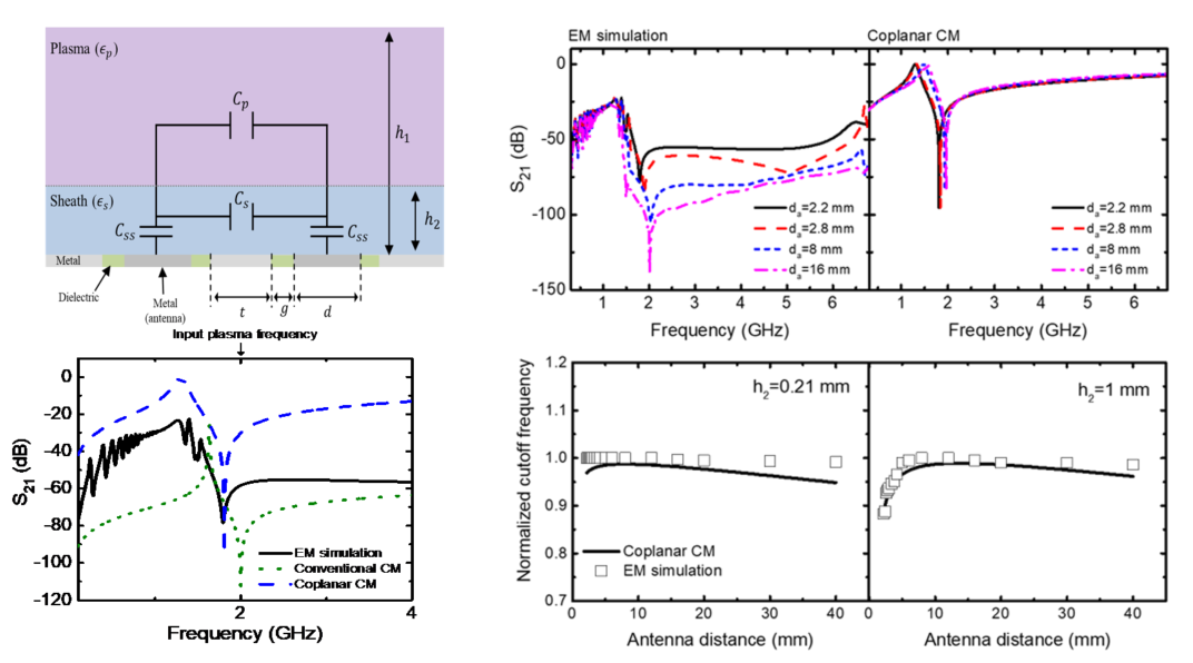
▲ Images of modeling, theoretical calculation, and experimental verification of plasma density measurement
Senior research scientist Hyo-chang Lee and Principal research scientist Jung-hyung Kim of the Advanced Instrumentation Institute of KRISS became the world’s first to develop the density measurement technology to directly measure plasma parameters. This technology is capable of real-time measurement of the density and uniformity values of plasma that directly affect the wafer process outcome, with the world’s top inaccuracy rate of 2% or lower.
The KRISS research team selected point-type, ring-type, and bar-type structures to develop the sensor and, based on the theoretical calculation and experiment regarding signal sensitivity and resonance properties, concluded that the bar-type flat sensor is the best structure. Later, the team comprehensively evaluated the sensor’s measurement reliability through a flat probe experiment, electromagnetic field simulation, and circuit model development.
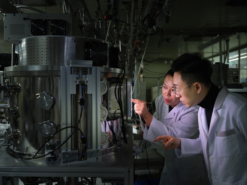
▲ Senior research scientist Hyo-chang Lee of KRISS (left) is conducting plasma experiment.
“The recently developed sensor is practical as it can be installed wherever desired, such as the electrostatic chuck, which is the bottom of the wafer, or edge rings and chamber walls,” said Dr. Hyo-chang Lee. “By establishing the standard test process for related technologies, we will use this plasma sensor technology for the reference equipment sensor for plasma measurement to verify performance of not only the semiconductors and display materials and parts, but also the semiconductors and display processing equipment applicable to etching, deposition, implantation, ashing, and sputtering. Through this sensor, it will be possible to develop intelligent plasma processing equipment for the next-generation semiconductor and display process.”
The research result was published in Plasma Sources Science and Technology, a world renowned plasma science journal.
In May, Dr. Hyo-chang Lee received the Noah Hershkowitz Early Career Award, which is granted only to one person each year, for his contribution to plasma measurement science and was appointed to the Editorial Board of Plasma Sources Science and Technology.